- 您现在的位置:买卖IC网 > Sheet目录2000 > IDT5V41066PGG (IDT, Integrated Device Technology Inc)IC CLK GEN SPRED SPECTRM 20TSSOP
IDT5V41066
4 OUTPUT PCIE GEN1/2 SYNTHESIZER
IDT 4 OUTPUT PCIE GEN1/2 SYNTHESIZER
6
IDT5V41066
REV D 112211
Layout Guidelines
Common R ecommendations for Differential Routing
D imension or Value
Unit
Figure
L1 length, route as non-coupled 50ohm trace
0.5 max
inch
1
L2 length, route as non-coupled 50ohm trace
0.2 max
inch
1
L3 length, route as non-coupled 50ohm trace
0.2 max
inch
1
Rs
33
ohm
1
Rt
49.9
ohm
1
Down Device Differential Routing
L4 length, route as coupled microstrip 100ohm differential trace
2 min to 16 max
inch
1
L4 length, route as coupled stripline 100ohm differential trace
1.8 min to 14.4 max
inch
1
Differential Routing to PCI Express Connector
L4 length, route as coupled microstrip 100ohm differential trace
0.25 to 14 max
inch
2
L4 length, route as coupled stripline 100ohm differential trace
0.225 min to 12.6 max
inch
2
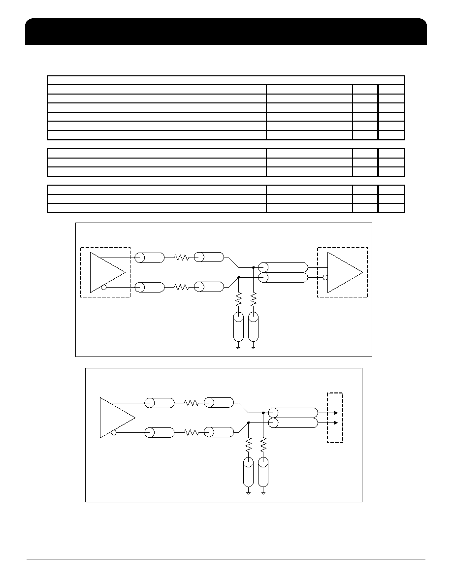
SRC Reference Clock
HCSL Output Buffer
L1
L1'
Rs
L2
L2'
Rs
L4'
L4
L3
L3'
Rt
PCI Express
Down Device
REF_CLK Input
Figure 1: Down Device Routing
HCSL Output Buffer
L1
L1'
Rs
L2
L2'
Rs
L4'
L4
L3
L3'
Rt
PCI Express
Add-in Board
REF_CLK Input
Figure 2: PCI Express Connector Routing
发布紧急采购,3分钟左右您将得到回复。
相关PDF资料
IDT5V49EE901NLGI8
IC PLL CLK GEN 200MHZ 32VFQFN
IDT5V49EE902NLGI
IC CLOCK GEN PLL 500MHZ 32VFQFPN
IDT5V49EE904NLGI8
IC PLL CLK GEN 200MHZ 32VFQFN
IDT821024PPG
IC PCM CODEC QUAD NONPROG 44TQFP
IDT821034DNG
IC PCM CODEC QUAD MPI 52-PQFP
IDT821054PQF
IC PCM CODEC QUAD MPI 64-PQFP
IDT82V3001APVG8
IC PLL WAN W/SGL REF INP 56-SSOP
IDT82V3010PVG
IC PLL WAN 51/E1/OC3 DUAL 56SSOP
相关代理商/技术参数
IDT5V41066PGG8
制造商:Integrated Device Technology Inc 功能描述:IC CLK GEN SPRED SPECTRM 20TSSOP
IDT5V41066PGGI
功能描述:IC CLOCK SYNTHESIZER 20TSSOP RoHS:是 类别:集成电路 (IC) >> 时钟/计时 - 专用 系列:- 标准包装:1 系列:- 类型:时钟/频率发生器,多路复用器 PLL:是 主要目的:存储器,RDRAM 输入:晶体 输出:LVCMOS 电路数:1 比率 - 输入:输出:1:2 差分 - 输入:输出:无/是 频率 - 最大:400MHz 电源电压:3 V ~ 3.6 V 工作温度:0°C ~ 85°C 安装类型:表面贴装 封装/外壳:16-TSSOP(0.173",4.40mm 宽) 供应商设备封装:16-TSSOP 包装:Digi-Reel® 其它名称:296-6719-6
IDT5V41066PGGI8
制造商:Integrated Device Technology Inc 功能描述:IC CLK GEN SPRED SPECTRM 20TSSOP
IDT5V41067APGG
功能描述:IC BUFFER MUX 2:4 20TSSOP RoHS:是 类别:集成电路 (IC) >> 时钟/计时 - 专用 系列:PCI Express® (PCIe) 标准包装:1 系列:- 类型:时钟/频率发生器,多路复用器 PLL:是 主要目的:存储器,RDRAM 输入:晶体 输出:LVCMOS 电路数:1 比率 - 输入:输出:1:2 差分 - 输入:输出:无/是 频率 - 最大:400MHz 电源电压:3 V ~ 3.6 V 工作温度:0°C ~ 85°C 安装类型:表面贴装 封装/外壳:16-TSSOP(0.173",4.40mm 宽) 供应商设备封装:16-TSSOP 包装:Digi-Reel® 其它名称:296-6719-6
IDT5V41067APGG8
制造商:Integrated Device Technology Inc 功能描述:IC CLK MUX PCIE 2 TO 4 20TSSOP
IDT5V41067APGGI
制造商:Integrated Device Technology Inc 功能描述:IC CLK MUX PCIE 2 TO 4 20TSSOP
IDT5V41067APGGI8
制造商:Integrated Device Technology Inc 功能描述:IC CLK MUX PCIE 2 TO 4 20TSSOP
IDT5V41068APGG
功能描述:IC CLK DVR MUX 2:1 16TSSOP RoHS:是 类别:集成电路 (IC) >> 时钟/计时 - 专用 系列:PCI Express® (PCIe) 标准包装:1 系列:- 类型:时钟/频率发生器,多路复用器 PLL:是 主要目的:存储器,RDRAM 输入:晶体 输出:LVCMOS 电路数:1 比率 - 输入:输出:1:2 差分 - 输入:输出:无/是 频率 - 最大:400MHz 电源电压:3 V ~ 3.6 V 工作温度:0°C ~ 85°C 安装类型:表面贴装 封装/外壳:16-TSSOP(0.173",4.40mm 宽) 供应商设备封装:16-TSSOP 包装:Digi-Reel® 其它名称:296-6719-6